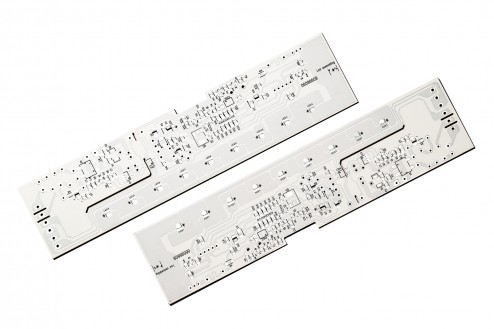
Cem 3 ht FR4 HTC
These are a valid alternative to aluminium substrates, with lower costs and the possibility of having a PCB with high dissipation capacity and metallized holes.
| CEM3 PCB REQUIREMENTS | CHARACTERISTICS |
| Number of layers | 1, 2 |
| Base material and thickness |
CEM-3 - thickness 1.6 mm |
| Thermal coefficient | 0.8 – 1.0 – 1.2 W/m°K |
| Min. track width/spacing | 0.200 mm |
| Insulation | 0.150 mm |
| Hole diameter | 0.200 mm |
| Base copper foil | 35μm / 1 ounce |
| Surface finish | Chemical Silver (AG) |
| Solder mask | Green, red, blue, black, yellow, transparent, white and high-reflectance white for LEDs |
| Silkscreen symbol colour | Green, red, blue, black, yellow, white |
| Minimum clearance between individual circuits shaped with a milling machine and/or arranged in a panel | > 2.0 mm (CNC shaping) |
| Minimum clearance between the outermost tracks for cutting circuit panel by means of V-cut scoring | > 0.4 mm with V-cut scoring |
| Production tests | Design Rule Check (DRC) |
| Electrical testing | Standard for all PCBs |
